|
Product Details:
|
| Product Name: | Mos Field Effect Transistor | V DSS Drain-Source Voltage: | -60 V |
|---|---|---|---|
| V GSS Gate-Source Voltage: | ±20 V | T J Maximum Junction Temperature: | 175°C |
| T STG Storage Temperature Range: | -55 To 175 °C | I S Source Current-Continuous(Body Diode): | -40A |
| High Light: | logic mosfet switch,mosfet driver using transistor |
||
Custom Made Mos Field Effect Transistor With Low On State Resistance
Mos Field Effect Transistor Feature
-60V/-40A
R DS(ON) = 19mΩ(typ.)@V GS = -10V
R DS(ON) = 25mΩ(typ.)@V GS = -4.5V
100% avalanche tested
Reliable and Rugged
Halogen Free and Green Devices Available
(RoHS Compliant)
Mos Field Effect Transistor Applications
Power Management in DC/DC converter.
Load switching.
Motor control.
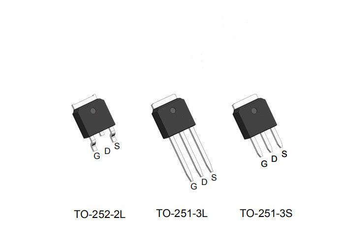
Ordering and Marking Information
D U V
G210P06 G210P06 G210P06
XYWXXXXXX XYWXXXXXX XYWXXXXXX
Package Code
D: TO-252-2L U: TO-251-3L V:TO-251-3S
Date Code
XYMXXXXXX
Note: HUAYI lead-free products contain molding compounds/die attach materials and 100% matte tin plateTermi-
Nation finish; which are fully compliant with RoHS. HUAYI lead-free products meet or exceed the lead-Free require-
ments of IPC/JEDEC J-STD-020 for MSL classification at lead-free peak reflow temperature. HUAYI defines “Green”
to mean lead-free (RoHS compliant) and halogen free (Br or Cl does not exceed 900ppm by weight in homogeneous
material and total of Br and Cl does not exceed 1500ppm by weight).
HUAYI reserves the right to make changes, corrections, enhancements, modifications, and improvements to this pr
-oduct and/or to this document at any time without notice.
Absolute Maximum Ratings
![]()
![]()
Contact Person: Mr. David Lee
Tel: +86 13417075252
Fax: 86-755-83232335